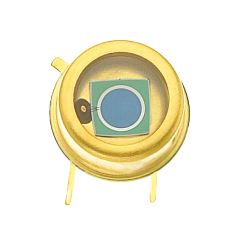
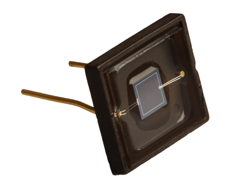
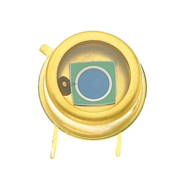
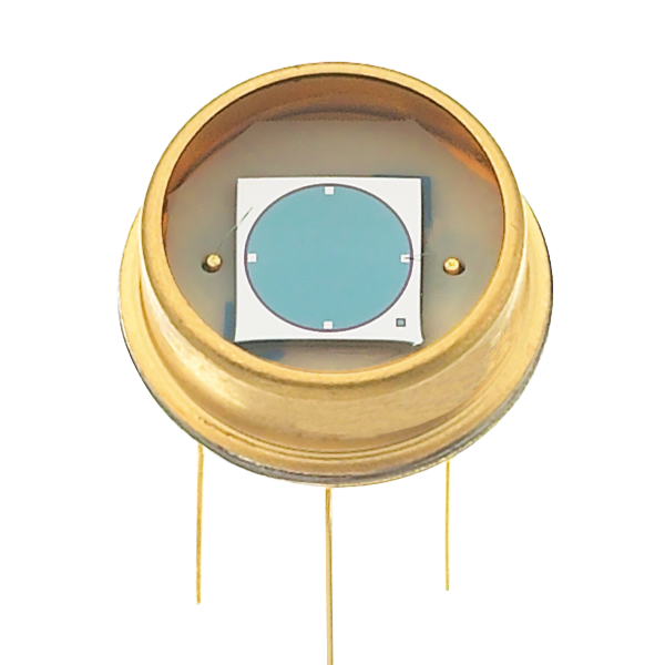
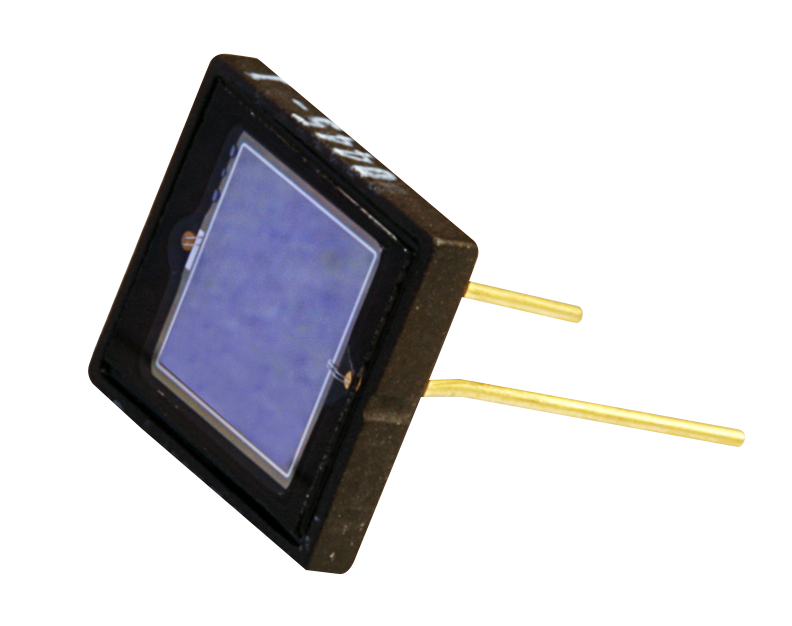
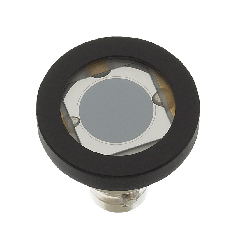
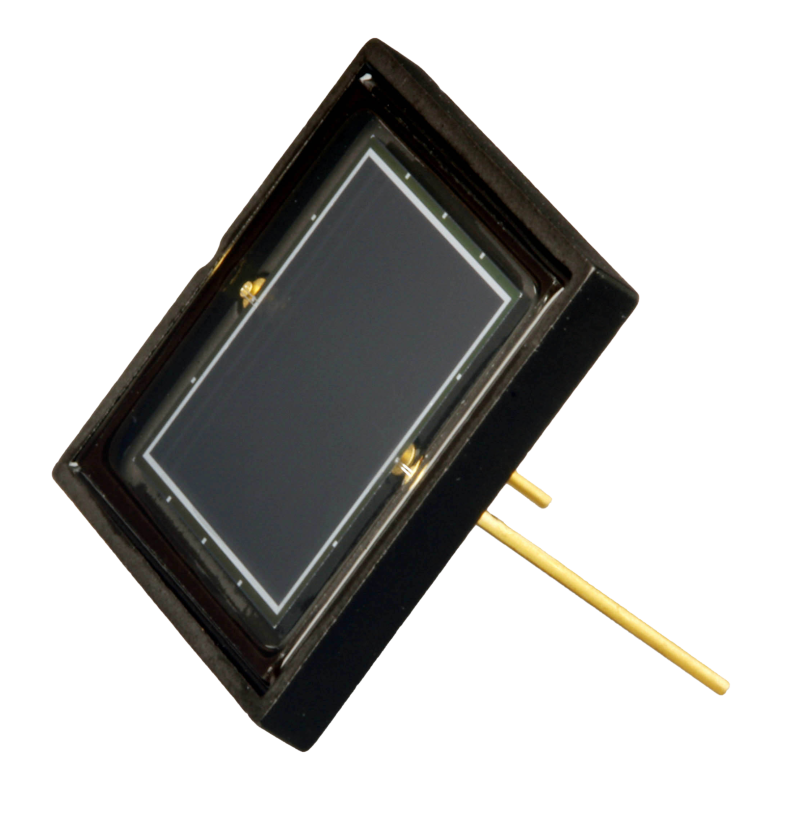
Planar Diffused Photodiodes

Inversion Layer, Metal Package §

OSI Optoelectronics offers two distinct families of UV enhanced silicon photodiodes. Inversion channel series and planar diffused series. Both families of devices are especially designed for low noise detection in the UV region of electromagnetic spectrum. Inversion layer structure UV enhanced photodiodes exhibit 100% internal quantum efficiency and are well suited for low intensity light measurements. They have high shunt resistance, low noise and high breakdown voltages. The response uniformity across the surface and quantum efficiency improves with 5 to 10 volts applied reverse bias. Photocurrent non-linearity sets in at lower photocurrents for inversion layer devices compared to the diffused ones. Below 700nm, their responsivities vary little with temperature.

Planar diffused structure (UV-D Series) UV enhanced photodiodes show significant advantages over inversion layer devices, such as lower capacitance and higher response time. These devices exhibit linearity of photocurrent up to higher response time. The devices exhibit linearity of photocurrent up to higher light input power compared to inversion layer devices. They have relatively lower responsivities and quantum efficiencies compared to inversion layer devices.

There are two types of planar diffused UV enhanced photodiodes available: UVD and UVE. Both series have almost similar electro-optical characteristics, except in the UVE series, where the near IR responses of the devices are suppressed. This is especially desirable if blocking the near IR region of the spectrum is necessary. UVD devices peak at 970 nm and UVE devices at 720 nm (see graph). Both series may be biased for lower capacitance, faster response and wider dynamic range. Or they may be operated in the photovoltaic (unbiased) mode for applications requiring low drift with temperature variations. The UVE devices have a higher shunt resistance than their counterparts of UVD devices, but have a higher capacitance. These detectors are ideal for coupling to an OP-AMP in the current mode configuration as shown above.

Silicon Planar Diffused

Product Applications

  • Pulse Detectors
  • Optical Communications
  • Bar Code Readers
  • Optical Remote Control
  • Medical Equipment
  • High Speed Photometry

Product Features

  • High Speed Response
  • Low Capacitance
  • Low Dark Current
  • Wide Dynamic Range
  • High Responsivity

'UVD' Series Planar DIffused, Metal Packages

Model Number Active Area Active Area Dimension Peak Wavelength Responsivity @ 254nm Capacitance Shunt Resistance Rise Time Package Click Image to Zoom
UV-005D 5.7 mm² 2.4 sq 970 0.10 A/W 100pF 4 MΩ 0.10 µs 5 / TO-5 No image found for (UV-005D)
UV-013D 13 mm² 3.6 sq 970 nm 0.10 A/W 225 pF 2 MΩ 0.2 µs 5 / TO-5 Click to View Larger Image of (UV-013D)
UV-035D 34 mm² 5.8 sq 970 nm 0.10 A/W 550 pF 0.50 MΩ 0.4 µs 6 / TO-8 Click to View Larger Image of (UV-035D)
OSD1.2-7U(Q) 1.2 mm² 1.1 sq 970 nm 0.10(0.12) A/W 40 pF 5 GΩ 0.1 µs 7 / TO-18 Click to View Larger Image of (OSD1.2-7U(Q))
OSD5.8-7U(Q) 5.8 mm² 2.4 sq 970 nm 0.10(0.12) A/W 180 pF 3 GΩ 0.4 µs 5 / TO-5 Click to View Larger Image of (OSD5.8-7U(Q))
OSD35-7Q 33.6 mm² 5.8 sq 970 nm 0.12 A/W 1000 pF 0.50 GΩ 2 µs 3 / TO-8 Click to View Larger Image of (OSD35-7Q)
OSD35-7CO 33.6 mm² 5.8 sq 970 nm 0.12 A/W 1000 pF 0.50 GΩ 2 µs 3 / TO-8 Click to View Larger Image of (OSD35-7CO)

'UVD' Series Planar DIffused, Ceramic Packages

Model Number Active Area Active Area Dimensions Peak Wavelength Responsivity @ 254nm Capacitance Shunt Resistance Rise Time Package Click Image to Zoom
UV-005DC 5.7 mm² 2.4 sq 970 nm 0.10 A/W 100 pF 4 MΩ 0.1 µs 25 / Ceramic Click to View Larger Image of (UV-005DC)
UV-35DC 34 mm² 5.8 sq 970 nm 0.10 A/W 550 pF 0.50 MΩ 0.4 µs 25 / Ceramic Click to View Larger Image of (UV-35DC)
UV-100DC 100 mm² 10 sq 970 nm 0.10 A/W 1750 pF 0.20 MΩ 1 µs 25 / Ceramic Click to View Larger Image of (UV-100DC)

(New Product) 'UVDQ', Metal Package, Quartz Window

Model Number Active Area Active Area Dimension Peak Wavelength Responsivity @ 200nm Capacitance Shunt Resistance Rise Time Package Click Image to Zoom
UV-005DQ 5.7 mm² 2.4 sq 980 nm 0.12 A/W 65 pF 1 GΩ 0.2 µs 2 / TO-5 No image found for (UV-005DQ)
UV-013DQ 13 mm² 3.6 sq 980 nm 0.12 A/W 150 pF 0.8 GΩ 0.5 µs 2 / TO-5 No image found for (UV-013DQ)
UV-035DQ 34 mm² 5.8 sq 980 nm 0.12 A/W 380 pF 0.1 GΩ 1 µs 3 / TO-8 No image found for (UV-035DQ)
UV-100DQ 100 mm² 10 sq 980 nm 0.12 A/W 1100 pF 0.2 GΩ 3 µs 10 / BNC No image found for (UV-100DQ)

(New Product) 'UVDQC', Ceramic Package, Quartz Window (New Product)

Model Number Active Area Active Area Dimension Peak Wavelength Responsivity @ 200nm Capacitance Shunt Resistance Rise Time Package Click Image to Zoom
UV-005DQC 5.7 mm² 2.4 sq 980 nm 0.12 A/W 65 pF 1 GΩ 0.2 µs 4 / Ceramic No image found for (UV-005DQC)
UV-035DQC 34 mm² 5.8 sq 980 nm 0.12 A/W 380 pF 0.4 GΩ 1 µs 4 / Ceramic No image found for (UV-035DQC)
UV-100DQC 100 mm² 10 sq 980 nm 0.12 A/W 1100 pF 0.2 GΩ 3 µs 4 / Ceramic No image found for (UV-100DQC)

(New Product) 'UVDK', Metal Package, Borosilicate Window¶ (New Product)

Model Number Active Area Active Area Dimension Peak Wavelength Responsivity @ 633nm Capacitance Shunt Resistance Rise Time Package Click Image to Zoom
UV-005DK 5.7 mm² 2.4 sq 980 nm 0.33 A/W 65 pF 1 GΩ 0.2 µs 2 / TO-5 No image found for (UV-005DK)
UV-013DK 13 mm² 3.6 sq 980 nm 0.33 A/W 150 pF 0.8 GΩ 0.5 µs 2 / TO-5 No image found for (UV-013DK)
UV-035DK 34 mm² 5.8 sq 980 nm 0.33 A/W 380 pF 0.4 GΩ 1 µs 3 / TO-8 No image found for (UV-035DK)
UV-100DK 100 mm² 10 sq 980 nm 0.33 A/W 1100 pF 0.2 GΩ 3 µs 10 / BNC No image found for (UV-100DK)
¶) Sensitivity range: 320-1100 nm
Q) Indicates Quartz Window
U) UV Transmitting Glass