Knowledgebase
For over 40 years OSI Optoelectronics has developed and manufactured OEM and custom solutions for leading technologies and industries.
If you have require any technical support, please visit our Support page.
For over 40 years OSI Optoelectronics has developed and manufactured OEM and custom solutions for leading technologies and industries.
If you have require any technical support, please visit our Support page.
Photodetectors last for an indefinite period of time when used properly and within the specified specifications. However, certain applications may put the photodiodes through optical, electrical, mechanical and/or thermal stresses beyond the specified ranges, and therefore limit their useful life.
In hermetically sealed detectors, such as TO metal packages, the responsivity is not expected to change over time. In non-hermetically sealed devices, however, the atmospheric contaminants as well as humidity may be diffused into the active area and result in trapping centers causing a short in the junction.
The surface dark current component can change over time due to ambient moisture. It is also susceptible to surface cleanness, surface contamination, i.e. sodium from hand grease could increase the dark current significantly. The bulk dark current should not increase over time.
Photodiode operates as a voltage source as well a current source in response to the incident light in the wavelength range of 200 nm to 1100 nm. The current measurement is preferred since the output current changes linearly with incident light power. The voltage output, however, changes logarithmically with incident light power.
Typically it is linear from a few pico-amps up to few milli-amps.
The dynamic range is the range of incident light power over which the current output from the photodiode is linearly related to the input power and is sometimes expressed in decibels: This range for a typical device is from 1 picowatt to 10 milliwatts, or 100 dB
The main difference between the two is the readout scheme of the output signal from each element in the linear array. In a Charge Coupled Device (CCD), the signal (charge) is transferred from one element to the next one down the row until it reaches the end, where it is read in sequence in a time multiplexed fashion. In a photodiode array (PDA), the signal (current) is outputted at each element's unique anode and cathode. Therefore, the signal for the PDA can be read simultaneously, rather than sequentially and multiplexed.
Responsivity matching from device to device for our catalog items is specified with 10%.
OSI Optoelectronics, for an additional fee, can provide responsivity matching photodiodes within a specified tolerance at a particular wavelength. Contact the Applications Group for your specific requirements.
No. Irradiated light on the non-active area adjacent to an active area may generate a small photocurrent in the detector. The magnitude of this signal is dependent of many parameters such as the wavelength of the radiation, the applied bias, and the amount of incident light on the active area as well as distance from the active area.
The silicon non-active area also absorbs light and contributes to the total photocurrent. If this contribution is not desired, a metal shield and/or a black polyamide layer can be put on the non-active area as a part of the semiconductor wafer process.
In the photovoltaic mode, the photodiode is neither operated with nor biasing. It is simply acting like a solar call, which converts light into electricity. In the Photoconductive mode, however, the photodiode can be Reversed Biased by voltages up to the specified maximum reverse voltage.
Applying a reverse bias in the PC mode introduces additional noise current to the generated photocurrent, therefore, reducing the signal to noise ratio. Hence, consider using operating the photodiode in PC mode for high speed applications (greater than 350 kHz) and/or in applications that require a wide dynamic range. For weak signal detection the PV mode is the preferred mode of operation.
Reverse biasing a photodiode is accomplished by setting the cathode of the detector at a higher electric potential than the anode's. In another words, applying a negative voltage to anode.
A photodiode is non-linear when an increase or decrease in the amount of incident light power does not generate an equal amount of photocurrent in the same photodiode with a tolerance of +/- 1%. This is the range where responsivity remains constant within +/-1%. That is: Above this range, also called dynamic range, the device may saturate completely at any incident light power level.
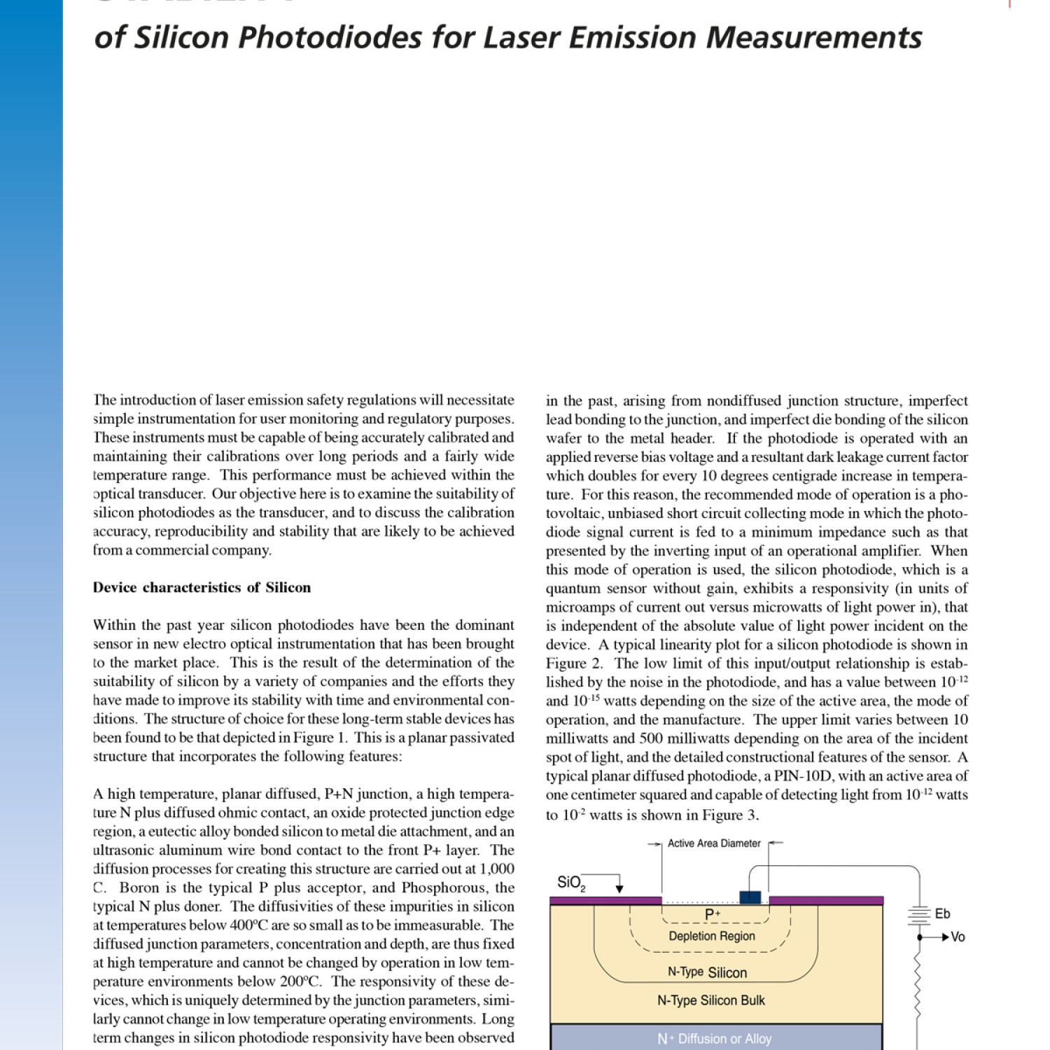
The maximum light power receivable by the detector before it saturates depends on the photodiode itself, the reverse voltage applied Vbias (Volts), and the resistance R (Ohms) of the circuit in which the detector is used and the wavelength used. The maximum photocurrent created in the linear range is Imax = Vbias / R (A mperes) and the corresponding Optical power is given by: Pmax = Imax / Rl (Watts) where Rl is the responsivity of the photodiode and varies with the wavelength. In the Photovoltaic (PV) mode, the previous definition is still correct but the voltage to consider is the silicon built-in value Built-in = 0.3 Volt. In the Photoconductive (PC) mode, the reverse voltage can reach up to 30 Volts (depending on the device). It is easy to understand that PC mode photodiodes have a wider dynamic range. To give an idea, Max is between 1 and 100 milliwatts.
Once the Saturation point is reached, the behavior of the photodiode becomes more and more non-linear until the Damage threshold point is reached. At this point the photodiode is no longer able to turn excess in incident optical power into a photocurrent output and all the extra energy received by the device would be absorbed, typically as heat. This heat inside the device can easily damage it irreversibly as it endangers the fragile wire bonds on the surface of the photodiode.
To reduce the light intensity received by the photodiode, one could use optical instruments such as beam splitters, filters or polarizers placed on the optical path between the source and the detector.
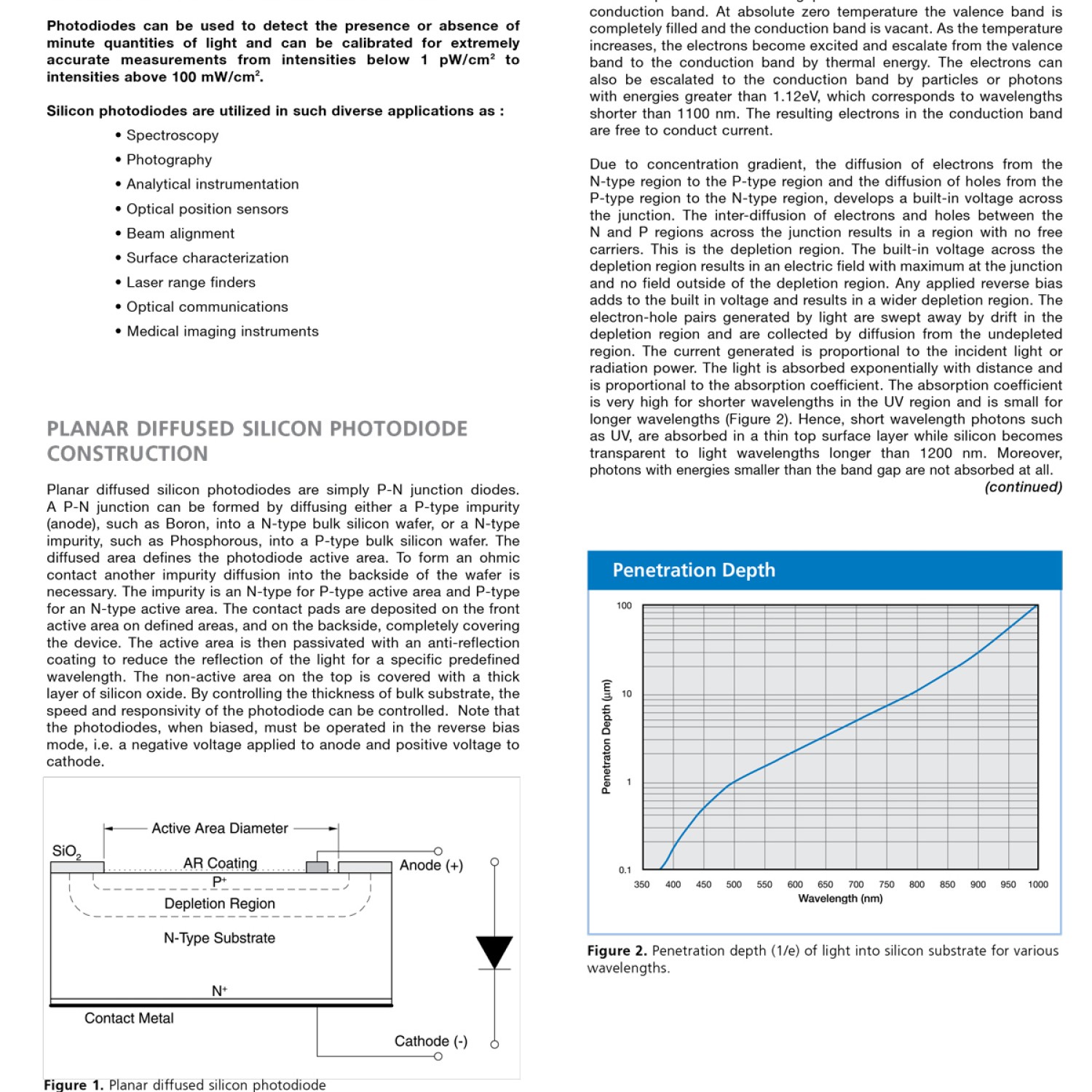
In silicon, the absorption coefficient increases with the temperature. If the temperature goes up, the absorption depth of light decreases. As a consequence, the responsivity for short wavelengths has a negative temperature coefficient, since a significant amount of carriers could recombine and get lost in the heavily doped p+ layer. For the longer wavelengths, responsivity has a positive temperature coeffcient, since more carriers will be generated in or near the depletion region of the pn junction, and participate in the photocurrent by increasing it.
Drift current is the dominating current (dark current) in Photoconductive (PC) mode and varies directly with the temperature. In Photovoltaic (PV) mode, the diffusion current is the dominating current, which determines the Shunt resistance. It varies as square of the temperature. Thus the change in temperature affects the photodetector more in photovoltaic mode than in photoconductive mode of operation. In general, in PC mode of operation, dark current may approximately double for every 10°C increase in temperature. In PV mode of operation, however, shunt resistance may approximately double for every 6°C decrease in temperature. The exact change is dependent on additional parameters such as the applied reverse voltage, the bulk resistivity as well as the thickness of the bulk substrate.
Since noise currents are generated as result of dark current (shunt resistance), the higher the temperature, the higher the noise in the detector. As a consequence, VB (breakdown voltage) decreases as the temperature increases.
The human eye senses both brightness and color and its response vary as a function of the wavelength. A color model based on human perception developed by the Commission Internationale de l'Eclairage, (the International Commission on Illumination) committee.
PIN-10AP is a detector / filter combination with a spectral response matching the CIE photopic spectrum. This detector is designed to have a spectral response like that of the human eye's visual response in the photopic region. This is the response of the eye with impinging intensities greater than about 0.1 Lux. In this region the eye response peaks at 555nm.
OSI Optoelectronics' proprietary designed AP filters are used in conjunction with a photodiode, accurately match the C.I.E. curve to within +/- 2% of area, as shown in the standard photodetector catalog.
Yes, optical calibration and also position linearity calibration for position sensing detectors.
It is the measurement of the response of a photodiode at various wavelengths. It is defined as responsivity vs. wavelength. Responsivity is measured in Amps / Watts except for PIN-10AP (C.I.E. human eye response), which can also be calibrated at color temperature of 2856 ºK (CIE standard Illuminant A) in both Amps/ Lux and the equivalent Amps / Foot-candle. If you have a specific requirements please contact one of our Applications Engineers.
No they are not. That procedure would delay the delivery of orders in an unacceptable way and would increase the cost to the customer. Responsivity of OSI Optoelectronics photodiodes is repeatable with high accuracy.
Yes, any of the devices can individually be calibrated if requested.
About 1-2 additional weeks.
Any photodiode (with or without optical filters) can be calibrated in house for responsivity from 400-1100 nm, 200-400 nm or combination of both (200-1100nm) in 10 nm steps. They can also be calibrated at a single wavelength. Contact one our inside representatives for pricing.
A table and a graph consisting of wavelengths versus responsivity, and a certification.
All optical calibrations performed by OSI Optoelectronics are NIST traceable and will be provided with a certification of compliance.
Various optical filters are available to meet specific application spectral requirements. Here are a few examples of the optical filter types available: - Shortpass filters (cut-off) transmit short wavelengths photons while blocking the longer wavelengths. - Longpass filters (cut-on) transmit long wavelength photons while blocking the shorter wavelengths. - Bandpass filters, combine a shortpass and a longpass filter property to transmit only a bandwidth of wavelengths. - Natural density filters attenuate light so that only a percentage of photons are transmitted. - Custom thin film coatings can be applied to either or both surface(s) of the filter glass to fine-tune the more stringent requirements if necessary.
Yes, anti-reflective coatings can be applied to either one or both sides of the glass to reduce glass reflection for a certain wavelength.
In very low light level applications, since a very large value feedback resistor is needed, there is Johnson current noise associated with the resistor, which reduces signal to noise ratio, which is undesirable. Silicon Avalanche Photodiodes (APDs) make use of internal multiplication instead to achieve gain. The gain is due to impact ionization. APDs are also useful when the amplifier noise is limiting.
TPDs internal gain is triggered by a high reverse bias (~200-300V usually). Due to high bias the resulting strong electric field energize the electrons with enough kinetic energy to generate more electrons by collision ionization and starting a ''chain reaction'', or ''avalanche'' process.
All of OSI Optoelectronics fiber optic detectors are available with a flat window, spherical micro lens (fish eye) window as well as any of the standard receptacles such as SMA, ST, FC, etc., for direct optical fiber coupling. Contact our Applications Group for further information.
The Photops™ Series combine either a Photoconductive or UV enhanced photodiode with an operational amplifier die in the same package.
By having a signal amplified as close to the detector as possible, the effects of noise picked by the pins, wire leads, and other PCB conductor traces can be minimized. This is in addition to saving a lot of space on your board or any other substrate.
Photops™ are very versatile components. They can be utilized for various gains and bandwidths determined by the external feedback components (resistors and capacitors). Since bandwidth and gain characteristics are application specific, adding a specific value resistor and/or capacitor will limit the operating of these devices.
Yes, any modification is possible. OSI Optoelectronics can not only provide any additional electrical components in the same package, but can also include an optical filter. Please contact our Applications Group with any of your specific requirements.
The feedback resistor, Rf, directly determines the gain in a transimpedance amplifier configuration; e.g. a 10kW resistor will amplify the signal, including noise, by a factor 10,000. The feedback capacitor, Cf, will determine the -3dB-frequency response as following: The Gain Bandwidth Product (GBP) of the op-amp limits the desired frequency response of the detector/amplifier combination. Rf and Cf should be chosen such that the -3dB frequency response to be less than the maximum frequency of the op-amp: where CA is the amplifier's input capacitance and CJ is the photodiode's junction capacitance. A large value RF, even though achieving a large gain, will reduce the bandwidth as well as introducing additional noise due to the thermal noise in the resistor. An increase of Cf, however, will increase the stability of the system, but at the expense of a slower response time.
The Transimpedance Amplifier (TIA) bandwidth is related to the load resistance per following relationship: where RL is the load resistance.
The Noise Equivalent Power or NEP, is the incident optical power, which generates a photocurrent equal to the noise of the photodiode. In other words, it is the optical power for which the Signal-to-Noise Ratio is equal to one. This value is used as the minimum detectable incident power.
Theoretically there is no lower limit for the optical power that a photodiode can detect. However, the dark current limits the minimum detectable optical power by reducing the signal to noise ratio to less than one.
Pn the photovoltaic mode measurements, the limiting source of noise is the Johnson (or thermal) noise in the source or shunt resistance. In other words shunt or source resistance is a noise-generating resistance. These are the charged particles produced as a result of the thermal energy in the resistance. This relation is given by: where kb is the Boltzman constant, T the temperature in Kelvin, Df the noise measurement bandwidth, and RSH the shunt resistance of the photodiode. In the Photoconductive mode, however, the dominant source of noise is the Shot noise and is related to dark current by: where IP is the photocurrent, ID the dark current, q the elementary charge and Df the noise measurement bandwidth.
Noise is the random electrical signal that interferes with the measurement of the signal of interest. Since both shot and Johnson noises are distributed over a wide frequency range, reducing the noise bandwidth effectively reduces the noise in the measurement. The high frequency noise cutoff point is approximately equal to the smallest of either: - p/2 times the upper 3 dB frequency limit of the analog DC measuring circuitry or - 0.55/tr where tr is the photodiode's 10%-90% rise time.
If not properly shielded, electromagnetic energy can be picked up at the pins of a device. Also, to a lesser extent, the same energy can come through unshielded windows.
No. In this series OSI Optoelectronics' propriety photodiode design make them less responsive in the near IR range of electromagnetic spectrum. The photodiodes are simply lying behind a quartz glass window.
No, because there would be a significant loss of XUV light through the window, due to absorption. XUV devices are shipped with removable can and window. The devices in this family have a higher output current from X-ray. X-ray photons tend to scatter as they pass through glass.
No. Though applying a reverse bias in excess of the maximum specified may result in permanent damage to the device.
The maximum reverse voltage that can be safely applied to XUV devices is 3 to 5 Volts.
XUV devices can detect X-ray energies up to 17.6 keV directly without using scintillation crystals.
No. For energies over 17.6 keV, an indirect measurement method by using scintillating crystals is recommended. You may contact our Applications Group for further information about your specific application.
Scintillating crystals are inorganic crystals, which convert X-ray photons to visible light by dominantly the scattering effect.
There are many scintillating crystals that can be used with photodiodes. Some of the most popular are: Cadmium Tungstate (CdWO4), Cesium Iodide (CsI) and Bismuth Germanate Oxide (BGO).
Since there are too many variables involved in designing a detector/crystal combination, please contact our Applications Group to discuss your specific application.
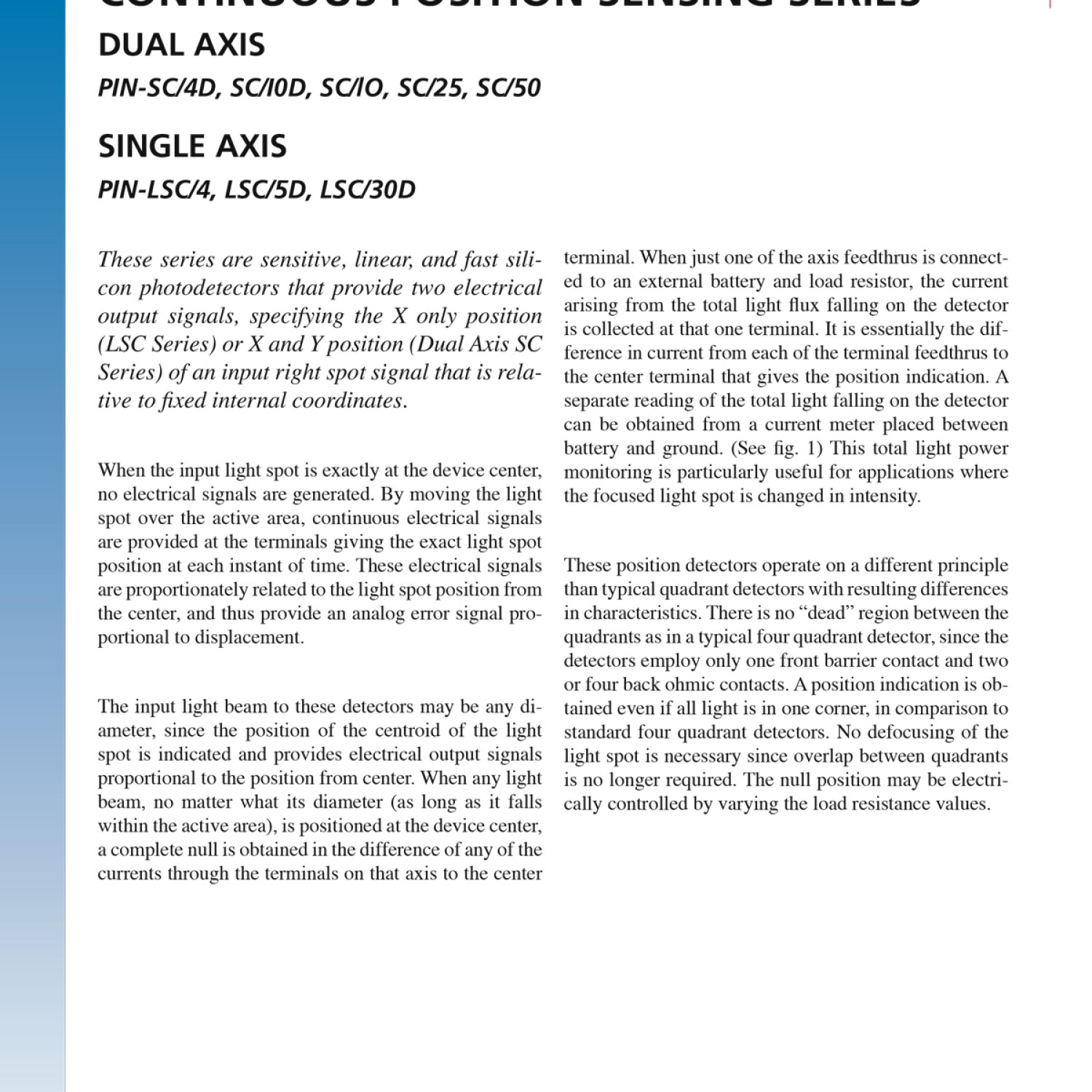
Position Sensing Devices, better known as PSDs, are single substrate photodiodes capable of finding or locating a beam within a defined sensing area. They are used in a variety of applications from human eye movement monitoring, mirrors or machine tool alignment to vibration analysis, beam position control and more.
Position Sensing Devices are divided into two families: the segmented PSDs and the lateral-effect PSD's.
Segmented PSDs are common substrate photodiodes divided into either two or four segments, separated by a gap or dead region. A symmetrical optical beam generates equal photocurrents in all segments, if positioned in the center.
Lateral PSDs are continuous single element planar diffused photodiodes with no gaps or dead areas. Theses types of PSDs provide direct readout of a light spot displacement across the entire sensing area.
Segmented PSDs offer position resolutions better than 0.1mm and accuracy higher than lateral effect PSDs due to superior responsivity match between elements. With S.N.R. (Signal to Noise Ratio) not effecting the resolution, very low light level detection is possible. They exhibit excellent stability over time and temperature and fast response times necessary for pulsed applications. They are excellent for nulling or beam centering applications. Lateral effect PSDs have a wide dynamic range, they can measure the light position all the way to the edge of the sensor. They are independent of the light spot profile and can resolve positions better than 0.5 mm. Their resolution is detector / circuit S.N.R. dependent.
OSI Optoelectronics manufactures two types of lateral effect PSDs. Duo-Lateral and Tetra-Lateral structures. Both structures are available in one and two-dimensional configurations.
In Duo-Lateral PSDs, there are two resistive layers, one at the top and the other at the bottom of the photodiode for two directional movements of X and Y. This type of structure can resolve light spot movements of less that 0.5 mm. They exhibit excellent position linearity over the entire active area. The Tetra-Lateral PSDs, however, consist of a single resistive layer, in which the photocurrent is divided in two or four parts for one or two-dimensional sensing respectively. They show smaller dark currents and faster response times compared to duo-lateral PSDs.
Position resolution is defined as the minimum detectable displacement of a spot of light on the detector active area.
Position Detection Error (PDE) or Accuracy is defined as the geometric variation between the actual position and the measured position of an incident spot of light. For all calculations, the zero is defined as the electrical center. This is the point at which I1=I2. The PDE is calculated as follows: where I1 and I2 are the photocurrents at the ends of the PSD, L is the sensing area half-length in mm, and X (mm) is the actual displacement of the light spot from the electrical center. PDE is smaller for a small active area device.
Position linearity refers to the accuracy of the measured position compared to the actual position of an incident light spot. Good position linearity means low Position Detection Error.
The position resolution depends on the light intensity, the detector/electronics noise and bandwidth. In lateral-effect PSDs, the position resolution is limited by the signal to noise ratio of the system. It varies from device to device; however, position resolutions in excess of one part in ten million have been achieved with OSI Optoelectronics lateral effect PSDs.
In the lateral-effect PSDs, the input light spot profile and intensity do not affect the accuracy of the devices. The incoming beam may be any size and shape, since the position of the centroid of the light spot is measured which provides output signals proportional to the displacement from the center.
In lateral effect PSDs, neither position resolution nor accuracy is dependent on the spot size. However, in segmented PSDs, the light spot has to overlap all segments at all times and it can not be smaller than the gap between the segments. Furthermore, in segmented PSDs, the position linearity is dependent on beam profile uniformity.
It could be related to fluctuations of the ambient temperature or instability of the power supply source.
Position Detection Error (PDE) does not change whether the device is operated in PV mode or PC mode. However, since Position resolution is SNR dependent, the additional dark current (shot noise) due to biasing does in fact reduce the resolution.
It is repeatable, but only within the maximum percentage specified for the device.
Similar to a regular photodiode applying a reverse bias reduces the rise time. Furthermore, it increases the high end of dynamic range.
The response uniformity between the segments is almost perfect with XX% maximum non-uniformity between the elements.
Crosstalk between the elements is affected by the gap size between the elements and the wavelength that's being measured. A larger gapsize will result in less cross talk and shorter wavelengths produce less crosstalk. Quantifiable results depend on the specific silicon device structure.
Since in segmented photodiodes the relative position of the spot is determined by the ration between the photocurrents, the accuracy and resolution does not depend on the photodiode dark current, as long as the signal to noise ratio is above one.
Since in segmented photodiodes the relative position of the spot is determined by the ration between the photocurrents, the accuracy and resolution does not depend on the photodiode dark current, as long as the signal to noise ratio is above one.
OSI Optoelectronics standard photodiodes are offered in three different types of packaging as well as chip only (solderable series):- Metal packages, including standard TO-18, TO-46, TO-5 and TO-8. - Plastic packages and - Mold packages
We do not recommend reflow soldering and vapor phase soldering for any of the package standard photodiodes. They can be either soldered by a soldering iron in circuit boards or sockets, or by dip soldering.
Open or exposed devices can absorb contaminants, such as ionized molecules in water, and "short" the diode junction by increasing the dark current. Excessive care must be taken when handling open devices. Handle chips with anti-static plastic tweezers or similar items.
Since most of OSI Optoelectronics standard photodiodes are either silicon or quartz, they can be cleaned with isopropyl alcohol and a soft optical grade pad.
Our standard products are usually centered within +/- 0.010 inches.
Usually +/- 1º.
Accuracy: A measure of the deviation in the output of a device from the actual or expected value.
Active Area (A.A.): Defined as the diffused area where the photodiode junction is active and can convert photons can generate current. Range: tens of mm sq. to a few cm sq.
Bandwidth (BW): A measure of the information-carrying capacity of a medium. Specifically, it is the frequency of a sinusoidal input light at which the output current of a photodiode falls to 70% of the output in DC mode. B = 0.35 / tr, where tr is the rise time. Range: a few kHz to over 1GHz.
Breakdown Voltage (VBR): A reverse bias voltage applied to a photodiode where a small change in voltage causes a relatively large change in current flowing through the diode. A photodiode gets damaged passed this point. Usually defined as the reverse bias for a dark current at 10 µA. Range: a few Volts to a few hundreds.
Junction Capacitance (CJ): A measure of the ability of the device to store an electric charge. Depends on the substrate resistivity, the reverse voltage, and the active area. Range : a few pF to a few tens of nF.
Damage threshold: Point after which an excess of incoming optical power can damage irreversibly the photodiode. Occurs after the saturation point.
Dark Current (ID): A small value current that flows in a photodiode while reversed biased, due to thermal generation of carriers and surface leakage with no incident light (also called leakage current). Range: a few pA to 10 m A.
Degradation: A drift in output for a detector submitted to a constant input optical power for a long period of time.
Drift: A change in output over time due to temperature or bias variations.
Dynamic Range: Range of input light intensity over which the responsivity is within linearity specification.
Fall Time, tf: The time for the output current of a photodiode to fall from 90% to 10% of initial level in response to an instantaneous fall in input light power. Range: Same as tr.
Filter: An optical component which allows a range of certain wavelengths to be transmitted. The medium of transmission can be glass, epoxy, plastic, etc.
Gain Bandwidth Product (GBP): The GBP is the frequency bandwidth of an operational amplifier with a gain of 1. As the gain (feedback resistance) increases, the bandwidth of the op-amp decreases, as the GBP keeps the same value. The GBP limits the behavior of the op-amp, as the maximum frequency is defined by :
Where Ca is the amplifier input capacitance, Cj the photodiode junction capacitance and Cf is the feedback capacitance in a transimpedance amplification mode. Range: from 0.5 Mhz to over 1 Ghz.
Incident Light: Amount of light falling on a detector's active area measured in watts per square centimeter (also called Irradiance or flux).
Linearity: Specifically, a measure of deviation in responsivity of a device over a range of input light power. In general, a measure of deviation of a curve from a straight line within 1% linearity (also called accuracy).
Noise Equivalent Power (NEP): Optical power necessary to create a photocurrent equal to the noise, to obtain a signal-to-noise ratio of 1. It depends on the noise current and the responsivity. Range: 10-15 to 10-11 W/ Sqrt (Hz).
Noise: Random fluctuation in a variable.
Noise bandwidth: Range of frequencies of noise that occur in a system.
Photoconductive mode (PC): Reverse biased mode of operation of a photodiode, in which lower capacitance and faster rise time are obtained. Generates more noise ( dark current ).
Photocurrent (IPH): Flow of current generated by a photodiode in response to an incident optical power. The absorbed photons generate free charge carriers that are collected within the device.
Photovoltaic Mode (PV): Unbiased mode of operation of a photodiode, preferred in low frequency (up to 350 MHz) as well as ultra low light level applications.
Quantum Efficiency (QE): Percentage of incident photons that generate electrons and hole that effectively participate in the photocurrent. Range: A few % to over 100 %.
Repeatability: The ability of a device to produce the same output reading when subject to same input applied consecutively over a short period of time (also called precision). Sometimes used to signify device to device variation in parameter.
Resistivity (ρ): Resistivity of material defines cincentration of carriers in the bulk substrate. Range: between 1 and tens of thousands Ohms-cm.
Resolution: The smallest incremental change in input that can be distinguished from the noise in the ouput.
Response Time: Time necessary for a device to begin changing its output in response to a variation in the input.
Responsivity (Rλ): The ratio of output current (in Amperes) to input light power (in Watts). It is a constant in the dynamic range, at a given wavelength. (also known as sensitivity). Range: from 0 and 1 A/W.
Rise Time (TR): The time for the output current of a photodiode to rise from 10% to 90% of final level in response to an instantaneous rise in input light power. Range: from a few ps to tens of ms.
Saturation: The point after which a change in input optical power does not produce the same amount of change in the output. It marks the end of the dynamic range, and the beginning of the saturation region.
Selectivity: The ability of a device to distinguish the signal from the background.
Sensitivity: A proportionality constant that relates the output of a sensor to the input.
Shot noise (ISH): Noise related to the statistical fluctuation in both the photocurrent and the dark current. It is the dominant noise in the photoconductive mode.
Shunt Resistance (RSH): In the photovoltaic mode, this resistance is a merit factor of the device. The higher it is, the lower the noise is. It is defined as the dark current at a reverse bias of 10 mV. Range: a few M-Ohm to tens of G-Ohm.
Span: Range of output over linearity range of input.
Stability: The ability of a device to produce the same output when subject to same input applied over a long period of time. Specific to photodetectors, a measure of the ability of the detector's responsivity not to drift over extended period of time (inverse of degradation).
Substrate: It is the material used to manufacture photodiodes. Usually slightly doped silicon wafers are used.
Thermal noise: All resistors have a thermal (or Johnson) noise associated with them, due to thermal generation of carriers.